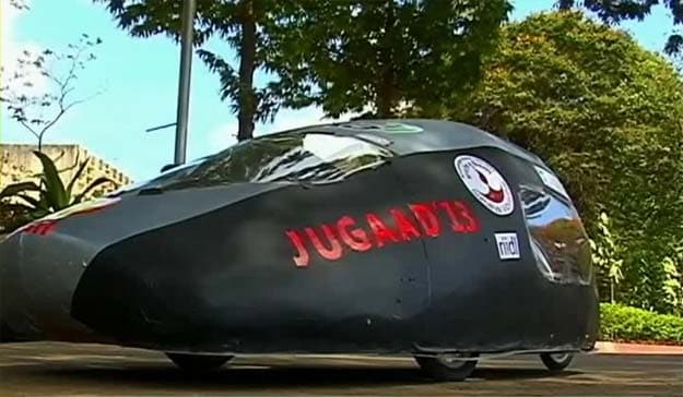
At a time when fuel prices are constantly rising and car companies are struggling with sales, this group of six students from Somaiya College in Mumbai has bunked a few classes, collected some scrap and put together a car that they claim does 300 km in a litre of petrol.
The vehicle is powered by a lawn mower engine and has only three wheels - two in the front and one at the rear.
"In our library was a book named 'Jugaad Innovation'. We were inspired by it. That's why we thought the name Jugaad would be apt for this car," said Kunal Jain, one of the students who worked on the car.
The fibre glass car, which weighs around 60 kg and cost around Rs. 4 lakh to build, has to be driven partly lying down, like in a race car.
"We would spend about 8-9 hours on this after college, sometimes bunk college to work on the designs. Then, we visited manufacturing units to get a basic idea," said Tony Thomas, a member of the design team.
The vehicle will now be showcased in Malaysia at the Shell Eco-marathon in July, where cars are judged by their fuel efficiency.
The Indian car market is dealing with its worst sales decline in history after sales in April fell for a sixth straight month as economic gloom and rising ownership costs savaged a once much-vaunted growth market. High interest rates and rising fuel costs didn't help their cause either. And seems like this bunch of bright students has found an answer to that.
This list is especially difficult because it requires 20/20 hindsight vision to see what gadgets will look like in the year 2020. Most of the time people try predicting future gadgets, they never end up coming close.
I mean, did anyone think that there would be something like the smartphone 10 years ago? Weren’t we supposed to have robots in our home and flying cars by now?
This is my attempt at trying to guess what gadgets will look like over the next decade, taking into account consumer trends, marketability, and current research and development on certain types of technology.
One of the more promising technologies in this decade is the use of touch technology. We can expect to see touch compatible interfaces everywhere; our cars, TV’s, watches, cameras, (insert any device with a screen here). I am particularly looking out for touch watches. Tissot made their Touch Watch a while ago and the new iPod shuffle can be turned into a touch watch with the corresponding watch band. Soon, we should expect to see touch watches on the market capable of supporting apps, WiFi, the weather, you name it. This technology will also travel to tables and other types of surfaces. Microsoft has recently developed a touch table called “Surface” which gives the user a touch interface on a table top that they provide (think the desk in Tron meets the Minority Report computers in the look and interface, respectively). The use of this technology should allow us to drop our smartphones and storage devices directly on the table and then load pictures, video, music, various types of files effortlessly while simultaneously browsing YouTube and checking our email. Check out this video from ASUS who takes this technology to a whole other level.
2. 3D Gaming
Think Xbox’s Kinect meets the 3D viewing experience we are used to seeing in films like Avatar. Or better yet, imagine virtual reality helmets that give the viewer a 3D mapping experience, combined with the technology of Kinect’s motion sensors. Either way, there is promise for the future of gaming with both motion detection and 3D viewing. Just using the Kinect technology alone, we could start to see something like the interface in the film “Minority Report” and would allow a gamer to precisely motion control their entire gaming experience. Hopefully, the price of 3D HDTV’s will drop so much so that the gaming industry starts to integrate more of that technology into their games. Regardless of price for now, the future of gaming looks bright, but my only reservation is if these gaming companies allow for advertisements during online multiplayer play because that would really ruin it on some level for me.
3. Heads Up Display (HUD) Technology
This one has to be my overall favorite pieces of tech that will be market bound in the not too distant future and in a decade from now, will hopefully be found everywhere. With this technology, lasers can project images up on a special glass surface to create what only fighter pilots have been able to see; colored graphics displayed on a windshield with a display of information. GM has had this technology in development for their cars for some time and they propose to display images on the windshield in front of the driver that display speedometer, RPM’s, temperature, along with outlines of the road or even 3D mapping of the surrounding environment. More applications of this technology are around the corner and might be found on our glasses or sunglasses, motorcycle helmets, or even mirrors. I like the idea of a bathroom mirror that can display the outside temperature, display your emails, a to-do list, and present the daily news headlines because we all need something better to look at than ourselves in the mirror while brushing our teeth. Check the video for a demonstration.
4. E-Paper and Flexible OLED Screens
Imagine a decade from now, waking up in the morning and getting ready for work. You go to your door to pick up the newspaper and low and behold it displays images and texts moving like a marquee across the surface of the paper. Perhaps something that looks like one of those newspapers from Harry Potter, e-paper and flexible OLED (Organic Light Emitting Diode) technology can present a digital media source on what looks like a piece of film. The bendable, lightweight paper should be recyclable or at least capable of updating itself with new information. This is just an example with newspapers. Now imagine a world where all of the paper we use, all of the screens we watch, were made out of OLED technology. The applications are practically limitless. And why not save a tree or two along the way…
5. Interconnectivity and “The Cloud”
OK, so this is not necessarily a gadget, but this technology proposes interconnectivity between all of your gadgets, computers, and the like, to create a seamless experience with your own sharing network. This technology also isn’t particularly new, Microsoft has created “Windows Azure” for small businesses, but requires more work in the areas speed, security, and stability. Cloud computing can take it to the next level in this decade and allow everyone everywhere to have their own “Cloud”. In 2020, we should be able to experience instant downloads and uploads in media sharing, file sharing, and preferences between all of our computers, gadgets, cars, smartphones, and maybe even our homes. We would never again have to worry about backing up our precious data, programs, and setup because our cloud will always have everything ready to go in a flash of lightning without the rain.
6. Health-Monitoring Gadgets
This piece of tech is interesting. I predict that by the year 2020 there will be an influx of portable or even disposable health monitoring gadgets that track a person’s blood pressure, heart rate, calories burned, stress levels, glucose levels, etc. It seems that this tech will come in the form of a patch or a bracelet, but it could come in other forms as well when applied on or implanted in your skin to give the user real time information about their body’s activities. This will be especially useful for people with health-related issues, but also for people who like to exercise (ok, maybe not like, but at least participate) and want to monitor their results. Perhaps using “The Cloud” will allow the future device to upload the results to your smartphone and email you suggestions to improve your health.
7. Voice Recognition
As of now, voice recognition is close to hitting it big time. It can be utilized on smartphones, computers, and even IBM’s “Watson,” which has the sophisticated capabilities to recognize speech patterns, natural language, and then analyze the data. Ten years from now, we could walk into a room and give a command for whatever we want from music, temperature control, light control, to perhaps even appliance and device control. In 2020, we should experience instantaneous responses to human voice commands in all of our devices at home. This tech may not only improve the quality of life for the blind and handicapped, but would also be really cool in general. We should just be sure not to name the system HAL (where each letter after them in the alphabet spells out I.B.M).
8. Night Vision Technology
Currently, you can buy infrared vision technology on some types of BMW models (5 & 7 Series) and is certainly promising for the future. Using my 2020 crystal ball, I can see most cars having the ability to switch from day vision to night vision either through the windshield or through a camera that gives a visible feed to a screen on the dash. Windshield night vision (similar to HUD tech and also similar to using OLED tech) can turn the night’s windy road ahead into the visible spectrum for drivers so that everything seems “lit up”. With the camera, a driver would be able to check the screen for anyone up ahead on dark, dirt road. Drivers would clearly see all other vehicles, obstacles, and most importantly, the road when traveling at night. If this technology becomes widespread in the car industry over the next decade, I would bet that nighttime accidents would decrease significantly.
9. Personal Motorized Vehicles
I’ve never had a problem with Vespa’s, scooters, Go/Mo-Peds and the like, but they really have left me unsatisfied as far as wanting one for personal use. I see that having one of these types of personal, compact “vehicles” is extremely useful in a city setting and if you are like me and are too lazy to ride a bike everywhere, your only options seem to be the Vespa route. However, the future looks promising for personal motorized vehicles and will likely see a big push in the upcoming decade. Everything from improvements to the Segway-type vehicle, the introduction of the YikeBike, or even the emergence of electric bicycles, will all likely be more common by the decade’s end along with other types of future looking personalized motorized vehicles.
Personally, I like the idea of the electric bike because of the fact that you can power the electric motor of the bike through a charge and by pedaling your way through traffic and are environmentally friendly.
10. Bye-Bye Camera?
For this last one, I am going to go against the grain a little and talk about a gadget that we will all might be waving “bye-bye” to in the near future. Ever since the introduction of a camera on the iPhone and other smartphones, digital photography has become even more portable and available in our daily lives. The technology has even gone further to include special applications to enhance user experience with special effects and editing. These smartphone companies are continuously figuring out ways to fit more megapixels on their phone’s cameras and third party peripherals are creating attachments like this one. Once they create a DSLR attachment, the personal digital camera may go the way of the Dodo bird, never to be seen again. This scenario might appear over the next decade simply because lugging around a redundant gadget will be inconvenient since your smartphone can capture HD pictures/HD video and then upload the media directly to your photo-sharing/video-sharing source.
So that’s the list. If you notice, I haven’t let my imagination run rampant because a lot of these technologies are close enough to making an impact on our daily lives sometime soon. With any luck, Nostradamus, Captain Hindsight, and the Mayans would all be proud of my future speculations and this is the best I can hope for when trying to guess the future of gadgets.
Designer Josselin Zaïgouche, who created the Zero Phone we’ve shown you half an year ago has now sent us an incredible design, the Apple Black Hole concept, possibly the iPhone of the year 2020. “What’s going to happen in 10 years” asks the designer and the answer should look something like this (click on images to enlarge):
As you can see, the Apple Black Hole comprises 4 components: the charging base, the Prism, the Black Hole and the giftbox. Things get interesting when you try to use the handset… its central ball will levitate when you open your hand and all functions will be controlled in mid-air, with the aid of holographic technology. How cool is that?
The Black Hole concept phone can be connected to the charging base and used as a desktop device, still projecting the needed interface. Brilliant? Yes! Viable? Maybe…
May 27, 2013 — Surprisingly the answer is yes. With the technology of today it is possible to use environmental friendly formic acid in fuel cell powering your mobile phone or laptop. Physicist Florian Nitze, Umeå University in Sweden, has in his thesis developed new catalysts to improve the capacity of these fuel cells.
Helical formed carbon nanofiber. (Credit: Image courtesy of Umeå University)
Fuel cells are different from batteries in that they require a constant source of fuel and oxygen to run. The technology is already commercially available but formic acid fuel cells still suffer from low power and lifetime.
The effect of a catalyst is to reduce the energy loss and to increase the rate of the chemical reactions, which leads to a higher efficiency in the fuel cell. In his thesis, Florian Nitze has developed new catalysts based on a combination of material science and nanotechnology -- engineering close to the atom level.
"Especially catalysts of palladium-nanoparticles attached to a unique helical formed carbon nanofibre proved to have a long lifetime and a very high potential to be used in formic acid fuel cells. The helical formed carbon nanofibre has a high electrical conductivity and a surface that is very easy to decorate with nanoparticles, "says Florian Nitze.
Several of the new catalysts that Florian Nitze have developed are based on palladium. It is a noble metal such as gold or platinum, but it is half as expensive.
Formic acid can be produced from renewable sources, i.e. wood, and is therefore a highly environmentally friendly alternative.
"One of the major advantages over Li-ion batteries, which are dominating the battery market, is that the charging only takes seconds by simple refueling with formic acid," says Florian Nitze.
Florian Nitze comes originally from Baden-Baden in Germany.
The working principle of a fuel cell: If for example hydrogen and oxygen (but equally valid for formic acid and oxygen) get in contact, they can burn and release a lot of energy. In this process hydrogen gives electrons to oxygen, it is oxidized whereas oxygen takes electrons from hydrogen, it is reduced.
The concept of a fuel cells is now to separate these two reaction spatially into two separate reactions, namely oxidation and reduction. The energy that would be released by burning can now be used as electric power if the two separated reactions are connected electrically. However, not all energy can be used; some energy is needed to keep the reaction running. Catalysts can lower this energy loss and speed up the reactions resulting in a higher efficiency of the fuel cell.
Cosmic Glitch: Astronomers Discover New Phenomenon in Neutron Star
May 29, 2013 — The physics behind some of the most extraordinary stellar objects in the Universe just became even more puzzling.
Artist's concept of a magnetar. These stellar remnants are the most magnetized objects in the cosmos. (Credit: NASA/Goddard Space Flight Center Conceptual Image Lab)
A group of astronomers led by McGill researchers using NASA's Swift satellite have discovered a new kind of glitch in the cosmos, specifically in the rotation of a neutron star.
Neutron stars are among the densest objects in the observable universe; higher densities are found only in their close cousins, black holes. A typical neutron star packs as much mass as half-a-million Earths within a diameter of only about 20 kilometers. A teaspoonful of neutron star matter would weigh approximately 1 billion tons, roughly the same as 100 skyscrapers made of solid lead.
Neutron stars are known to rotate very rapidly, from a few revolutions per minute to as fast as several hundred times per second. A neutron star glitch is an event in which the star suddenly begins rotating faster. These sudden spin-up glitches have long been thought to demonstrate that these exotic ultra-dense stellar objects contain some form of liquid, likely a superfluid.
This new cosmic glitch was detected in a special kind of neutron star -- a magnetar -- an ultra-magnetized neutron star that can exhibit dramatic outbursts of X-rays, sometimes so strong they can affect Earth's atmosphere from clear across the galaxy. A magnetar's magnetic field is so strong that, if one were located at the distance of the Moon, it could wipe clean a credit card magnetic strip here on Earth.
Now astronomers led by a research group at McGill University have discovered a new phenomenon: they observed a magnetar suddenly rotate slower -- a cosmic braking act they've dubbed an "anti-glitch." The result is reported in the May 30 issue ofNature.
The magnetar in question, 1E 2259+586 located roughly 10,000 light years away in the constellation of Cassiopeia, was being monitored by the McGill group using the Swift X-ray telescope in order to study the star's rotation and try to detect the occasional giant X-ray explosions that are often seen from magnetars.
"I looked at the data and was shocked -- the neutron star had suddenly slowed down," says Rob Archibald, lead author and MSc student at McGill University. "These stars are not supposed to behave this way."
Accompanying the sudden slowdown, which rang in at one third of a part per million of the 7-second rotation rate, was a large increase in the X-ray output of the magnetar, telltale evidence of a major event inside or near the surface of the neutron star.
"We've seen huge X-ray explosions from magnetars before," says Victoria Kaspi, Professor of Physics at McGill and leader of the Swift magnetar monitoring program, "but an anti-glitch was quite a surprise. This is telling us something brand new about the insides of these amazing objects." In 2002, NASA's Rossi X-ray Timing Explorer satellite also saw a large X-ray outburst from the source, but in that case, it was accompanied by a more usual spin-up glitch.
The internal structure of neutron stars is a long-standing puzzle, as the matter inside these stars is subject to forces so intense that they are presently not re-creatable in terrestrial laboratories. The densities at the hearts of neutron stars are thought to be upwards of 10 times higher than in the atomic nucleus, far beyond what current theories of matter can describe.
The reported anti-glitch strongly suggests previously unrecognized behaviour inside neutron stars, possibly with pockets of superfluid rotating at different speeds. The researchers further point out in the Nature paper that some properties of conventional glitches have been noted to be puzzling and suggestive of flaws in the existing theory to explain them. They are hoping that the discovery of a new phenomenon will open the door to renewed progress in understanding neutron star interiors.
The research was funded in part by the Natural Sciences and Engineering Research Council of Canada, the Canadian Institute for Advanced Research, the Fonds de recherche du Québec -- Nature et technologies, the Canada Research Chairs program, the Lorne Trottier Chair in Astrophysics and Cosmology, and the Centre de recherche en Astrophysique du Québec.
Crystal-Clear Method for Distinguishing Between Glass and Fluids
May 28, 2013 — Many solids are produced from melting. Depending on how quickly they cool off, invariably, internal tensile stresses begin to build up. One example are Prince Rupert's Drops, or Dutch tears: you can hit their thick end with a hammer without breaking them while a slight pressure applied to their thin end is enough to shatter the entire tear.
The colloids that were used for the model: particles, each with a diameter of approximately 150 nanometers, suspended in water. The solid nucleus consists of the plastic polystyrene, the surrounding shell of a thermosensitive poly(N-isopropyl-acrylamide) network. By lowering the temperature, each individual particle's volume - and, by definition, its packing density - can be increased. (Credit: Photo: HZB/M. Siebenbürger)
The properties of safety or even gorilla glass are determined to a large extent by their internal tensile stresses. However, until now, our understanding of the unique characteristics exhibited by the condition of the glass as compared with a tough molten mass was spotty at best. Now, a collaboration of several German and Cretian research teams has offered a surprisingly simple model to explain the difference between glass and molten materials.
The HZB's contribution was by chemist Dr. Miriam Siebenbürger of the Institute for Soft Matter and Functional Materials. Siebenbürger came up with a rather elegant model system consisting of spherical plastic particles in aqueous solution (a mixture known as a suspension). Due to the tiny size of the particles -- each having a diameter of around 150 nanometer -- they float in the aqueous solution but never sediment. The nanoparticles are covered by a thermosensitive "shell," whose thickness can be adjusted by varying the temperature, causing them to shrink and grow reversibly in a continuous manner. This allows the chemist to convert her samples from a densely packaged "glass" into a less dense, more fluid state, in other words melt them down. Through a series of rheological measurements, Miriam Siebenbürger was able to determine how quickly the internal tensions in her samples could relax at different particle packing densities.
For this purpose, she placed the samples in-between two parallel plates, which she counter-rotated relative to each other to produce shearing forces within the sample. After reaching a stationary state of shearing stress at a constant shearing rate, the rotating plates were actively stopped. Next, the force it takes to stop the plates to zero shear rate, and which is a gauge for internal tensions, was measured. In the process, the critical difference between the fluid and glassy state became apparent:
Whereas the fluid tensions dissipated without a trace, a proportion of the tensions was maintained in the glassy state. The results are fitting nicely into the theoretical model developed by a group of Constance physicists who calculated the behavior of hard spheres at different packing densities. What's more, measurements of the internal tensile stresses and dynamics of larger-sized particles (in the mm range) by Cretian and Düsseldorf researchers and the molecular dynamics simulation of hard spheres by a team of researchers from Cologne and Mainz exhibit similar patterns of behavior. The scientists are convinced that their findings apply to all types of glass that are created as a result of their high packing densities including metallic glass, which is mainly used for high-tech applications. The researchers' findings have now been published in the renowned scientific journal, Physical Review Letters and is selected as Focus in Physics" and "Editor's Suggestion."
Gold Nanocrystal Vibration Captured On Billion-Frames-Per-Second Film
May 23, 2013 — A billon-frames-per-second film has captured the vibrations of gold nanocrystals in stunning detail for the first time
The acoustic phonons can be visualized on the surface as regions of contraction (blue) and expansion (red). Also shown are two-dimensional images comparing the experimental results with theory and molecular dynamics simulation. The scale bar is 100 nanometers. (Credit: Jesse Clark/UCL)
The film, which was made using 3D imaging pioneered at the London Centre for Nanotechnology (LCN) at UCL, reveals important information about the composition of gold. The findings are published in the journalScience.
Jesse Clark, from the LCN and lead author of the paper said: "Just as the sound quality of a musical instrument can provide great detail about its construction, so too can the vibrations seen in materials provide important information about their composition and functions."
"It is absolutely amazing that we are able to capture snapshots of these nanoscale motions and create movies of these processes. This information is crucial to understanding the response of materials after perturbation. "
Scientists found that the vibrations were unusual because they start off at exactly the same moment everywhere inside the crystal. It was previously expected that the effects of the excitation would travel across the gold nanocrystal at the speed of sound, but they were found to be much faster, i.e., supersonic.
The new images support theoretical models for light interaction with metals, where energy is first transferred to electrons, which are able to short-circuit the much slower motion of the atoms.
The team carried out the experiments at the SLAC National Accelerator Laboratory using a revolutionary X-ray laser called the "Linac Coherent Light Source." The pulses of X-rays are extremely short (measured in femtoseconds, or quadrillionths of a second), meaning they are able to freeze all motion of the atoms in any sample, leaving only the electrons still moving.
However, the X-ray pulses are intense enough that the team was able to take single snapshots of the vibrations of the gold nanocrystals they were examining. The vibration was started with a short pulse of infrared light.
The vibrations were imaged a short time later in 3D using the coherent diffraction imaging methods pioneered in LCN by the Robinson group. The 3D movies reveal in exquisite detail the distortions taking place within the nanocrystal, with the fastest vibrations repeating every 90 picoseconds.
Professor Robinson, also from the LCN and the group leader, said: "This work represents an impressive example of teamwork by about a hundred people at SLAC. The SLAC linear accelerator was built in 1957 in direct response to the news of Sputnik.
"After compelling 50 years of sensational high energy physics, that machine has been refitted as a laser by the addition of a 100m long array of magnets. This 3km-sized machine produces a beam which is focused onto a crystal smaller than a micron in a pulse so short that all motion of its atoms is frozen still."
Stitching Defects Into World’s Thinnest Semiconductor
May 23, 2013 — In pioneering new research at Columbia University, scientists have grown high-quality crystals of molybdenum disulfide (MoS2), the world's thinnest semiconductor, and studied how these crystals stitch together at the atomic scale to form continuous sheets. Through beautiful images of strikingly symmetric stars and triangles hundreds of microns across, they have uncovered key insights into the optical and electronic properties of this new material, which can be either conducting or insulating to form the basic "on-off switch" for all digital electronics.
A false-color electron microscopy image showing the star-shaped crystals in monolayers of two-dimensional semiconducting molybdenum disulfide. The red, yellow, and blue colors represent two dominant crystal orientations that are stitched together by a line of atomic defects. (Credit: Image courtesy of Pinshane Y. Huang and David A. Muller
The study is published in the May 5, 2013, issue of Nature Materials.
"Our research is the first to systematically examine what kinds of defects result from these large growths, and to investigate how those defects change its properties," says James Hone, professor of mechanical engineering at Columbia Engineering, who led the study. "Our results will help develop ways to use this new material in atomically thin electronics that will become integral components of a whole new generation of revolutionary products such as flexible solar cells that conform to the body of a car."
This multidisciplinary collaboration by the Energy Frontier Research Center at Columbia University with Cornell University's Kavli Institute for Nanoscale Science focused on molybdenum disulfide because of its potential to create anything from highly efficient, flexible solar cells to conformable touch displays. Earlier work from Columbia demonstrated that monolayer MoS2 has an electronic structure distinct from the bulk form, and the researchers are excited about exploring other atomically thin metal dichalcogenides, which should have equally interesting properties. MoS2 is in a class of materials called transition metal dichalcogenides, which can be metals, semiconductors, dielectrics, and even superconductors.
"This material is the newest in a growing family of two-dimensional crystals," says Arend van der Zande, a research fellow at the Columbia Energy Frontier Research Center and one of the paper's three lead authors. "Graphene, a single sheet of carbon atoms, is the thinnest electrical conductor we know. With the addition of the monolayer molybdenum disulfide and other metal dichalcogenides, we have all the building blocks for modern electronics that must be created in atomically thin form. For example, we can now imagine sandwiching two different monolayer transition metal dichalcogenides between layers of graphene to make solar cells that are only eight atoms thick -- 20 thousand times smaller than a human hair!"
Until last year, the majority of experiments studying MoS2 were done by a process called mechanical exfoliation, which only produces samples just a few micrometers in size. "While these tiny specimens are fine for scientific studies," notes Daniel Chenet, a PhD in Hone's lab and another lead author, "they are much too small for use in any technological application. Figuring out how to grow these materials on a large scale is critical."
To study the material, the researchers refined an existing technique to grow large, symmetric crystals up to 100 microns across, but only three atoms thick. "If we could expand one of these crystals to the thickness of a sheet of plastic wrap, it would be large enough to cover a football field -- and it would not have any misaligned atoms," says Pinshane Huang, a PhD student in the David Muller lab at Cornell and the paper's third lead author.
For use in many applications, these crystals need to be joined together into continuous sheets like patches on a quilt. The connections between the crystals, called grain boundaries, can be as important as the crystals themselves in determining the material's performance on a large scale. "The grain boundaries become important in any technology," says Hone. "Say, for example, we want to make a solar cell. Now we need to have meters of this material, not micrometers, and that means that there will be thousands of grain boundaries. We need to understand what they do so we can control them."
The team used atomic-resolution electron microscopy to examine the grain boundaries of this material, and saw lines of misaligned atoms. Once they knew where to find the grain boundaries, and what they looked like, the team could study the effect of a single grain boundary on the properties of the MoS2. To do this, they built tiny transistors, the most basic component in all of electronics, out of the crystals and saw that the single, defective line of atoms at the grain boundaries could drastically change the key electronic and optical properties of the MoS2.
"We've made a lot of progress in controlling the growth of this new 'wonder' nanomaterial and are now developing techniques to integrate it into many new technologies," Hone adds. "We're only just beginning to scratch the surface of what we can make with these materials and what their properties are. For instance, we can easily remove this material from the growth substrate and transfer it on to any arbitrary surface, which enables us to integrate it into large-scale, flexible electronics and solar cells."
The crystal synthesis, optical measurements, electronic measurements, and theory were all performed by research groups at Columbia Engineering. The growth and electrical measurements were made by the Hone lab in mechanical engineering; the optical measurements were carried out in the Tony Heinz lab in physics. The structural modeling and electronic structure calculations were performed by the David Reichman lab in chemistry. The electron microscopy was performed by atomic imaging experts in the David Muller lab at Cornell University's School of Applied and Engineering Physics, and the Kavli Institute at Cornell for Nanoscale Science.
The study was sponsored by the Columbia Energy Frontier Research Center, with additional support provided by the National Science Foundation through the Cornell Center for Materials Research.
Innovation Could Bring Flexible Solar Cells, Transistors, Displays
May 22, 2013 — Researchers have created a new type of transparent electrode that might find uses in solar cells, flexible displays for computers and consumer electronics and future "optoelectronic" circuits for sensors and information processing.
Electron microscope images show a new material for transparent electrodes that might find uses in solar cells, flexible displays for computers and consumer electronics, and future "optoelectronic" circuits for sensors and information processing. The electrodes are made of silver nanowires covered with a material called graphene. At bottom is a model depicting the "co-percolating" network of graphene and silver nanowires. (Credit: Purdue University image/Birck Nanotechnology Center)
The electrode is made of silver nanowires covered with a material called graphene, an extremely thin layer of carbon. The hybrid material shows promise as a possible replacement for indium tin oxide, or ITO, used in transparent electrodes for touch-screen monitors, cell-phone displays and flat-screen televisions. Industry is seeking alternatives to ITO because of drawbacks: It is relatively expensive due to limited abundance of indium, and it is inflexible and degrades over time, becoming brittle and hindering performance.
"If you try to bend ITO it cracks and then stops functioning properly," said Purdue University doctoral student Suprem Das.
The hybrid material could represent a step toward innovations, including flexible solar cells and color monitors, flexible "heads-up" displays in car windshields and information displays on eyeglasses and visors.
"The key innovation is a material that is transparent, yet electrically conductive and flexible," said David Janes, a professor of electrical and computer engineering.
Research findings were detailed in a paper appearing online in April in the journal Advanced Functional Materials. It was authored by Das; visiting student Ruiyi Chen; graduate students Changwook Jeong and Mohammad Ryyan Khan; Janes and Muhammad A. Alam, a Purdue professor of electrical and computer engineering.
The hybrid concept was proposed in earlier publications by Purdue researchers, including a 2011 paper in the journal Nano Letters. The concept represents a general approach that could apply to many other materials, said Alam, who co-authored theNano Letters paper.
"This is a beautiful illustration of how theory enables a fundamental new way to engineer material at the nanoscale and tailor its properties," he said.
Such hybrid structures could enable researchers to overcome the "electron-transport bottleneck" of extremely thin films, referred to as two-dimensional materials.
Combining graphene and silver nanowires in a hybrid material overcomes drawbacks of each material individually: the graphene and nanowires conduct electricity with too much resistance to be practical for transparent electrodes. Sheets of graphene are made of individual segments called grains, and resistance increases at the boundaries between these grains. Silver nanowires, on the other hand, have high resistance because they are randomly oriented like a jumble of toothpicks facing in different directions. This random orientation makes for poor contact between nanowires, resulting in high resistance.
"So neither is good for conducting electricity, but when you combine them in a hybrid structure, they are," Janes said.
The graphene is draped over the silver nanowires.
"It's like putting a sheet of cellophane over a bowl of noodles," Janes said. "The graphene wraps around the silver nanowires and stretches around them."
Findings show the material has a low "sheet resistance," or the electrical resistance in very thin layers of material, which is measured in units called "squares." At 22 ohms per square, it is five times better than ITO, which has a sheet resistance of 100 ohms per square.
Moreover, the hybrid structure was found to have little resistance change when bent, whereas ITO shows dramatic increases in resistance when bent.
"The generality of the theoretical concept underlying this experimental demonstration -- namely 'percolation-doping' -- suggests that it is likely to apply to a broad range of other 2-D nanocrystaline material, including graphene," Alam said.
A patent application has been filed by Purdue's Office of Technology Commercialization.
May 22, 2013 — Researchers working to improve durability in fuel cell powered buses, including a team from Simon Fraser University, have discovered links between electrode degradation processes and bus membrane durability.
A team of SFU student researchers is at work at Ballard Power Systems in Burnaby carrying out tests to improve fuel cell durability. The study aims to make fuel-cell buses competitive with diesel hybrids. (Credit: Image courtesy of Simon Fraser University)
The team is quantifying the effects of electrode degradation stressors in the operating cycle of the bus on the membrane lifetime.
The findings of the study, led by SFU graduate student Natalia MaCauley, are the latest in a long-term study at Burnaby-based Ballard Power Systems and funded by Automotive Partnership Canada that aims to make fuel cell buses competitive with diesel hybrids.
To improve fuel cell module durability and predict longevity, researchers are studying the degradation mechanisms of the fuel cells that occur under real-world transit bus conditions.
Says SFU project lead Erik Kjeang: "Our strong multidisciplinary collaboration between chemistry and mechatronic systems engineering (MSE) is bearing fruit. The fuel cell is a mechatronic device, and the bandwidth of this project allows advances in chemistry to be engineered and implemented into Ballard's products."
Adds Ballard lead Shanna Knights: "We are pleased with the progress that our multidisciplinary team from SFU and UVic is making to develop improved membrane lifetimes for our next-generation fuel cell bus module and to understand the details of these complex failure mechanisms."
"With continued work, this research will permit significant product costs savings and improved fuel cell lifetimes so we can directly compete against incumbent diesel technology."
The research team, comprising 40 highly qualified personnel (HQPs) -- graduate students, undergraduate co-op students and post-doctoral fellows -- is also developing simulation tools that can eventually be used by industry partners in their testing protocols and operations of fuel cell buses.
SFU post-doctoral fellow Amir Niroumand, who heads the research on system level reliability and lifetime for fuel cell buses, says their objective is to operate fuel cells safely with extended lifetimes by studying how and why these fuel cells work.
"Our algorithms can be used for repair and maintenance, following through something like the check engine light in the car," explains Niroumand. "When onboard diagnostics indicate maintenance is required, the check engine light goes on and tells you to take the car to the shop; however, the car would not stop and would continue to operate. This requires the capability to detect potential issues and determine operating capabilities."
Ballard has been developing successive generations of products with improved durability for more than 15 years. Testing to improve the understanding of membrane failure mechanisms and validate developed predictive models is underway in labs at Ballard, SFU and UVic.
Project manager Kourosh Malek says the work to date has met all of its 18-month milestones, including a substantive effort devoted to training students. "This has formed an industry-driven platform for our hired HQPs," he says.
Kjeang adds: "This is not only research that will lower costs, extend product life and address sustainability issues. These HQPs, vital to the project, are creating tomorrow's workforce."
Stitching Defects Into World’s Thinnest Semiconductor
May 23, 2013 — In pioneering new research at Columbia University, scientists have grown high-quality crystals of molybdenum disulfide (MoS2), the world's thinnest semiconductor, and studied how these crystals stitch together at the atomic scale to form continuous sheets. Through beautiful images of strikingly symmetric stars and triangles hundreds of microns across, they have uncovered key insights into the optical and electronic properties of this new material, which can be either conducting or insulating to form the basic "on-off switch" for all digital electronics.
A false-color electron microscopy image showing the star-shaped crystals in monolayers of two-dimensional semiconducting molybdenum disulfide. The red, yellow, and blue colors represent two dominant crystal orientations that are stitched together by a line of atomic defects. (Credit: Image courtesy of Pinshane Y. Huang and David A. Muller
The study is published in the May 5, 2013, issue of Nature Materials.
"Our research is the first to systematically examine what kinds of defects result from these large growths, and to investigate how those defects change its properties," says James Hone, professor of mechanical engineering at Columbia Engineering, who led the study. "Our results will help develop ways to use this new material in atomically thin electronics that will become integral components of a whole new generation of revolutionary products such as flexible solar cells that conform to the body of a car."
This multidisciplinary collaboration by the Energy Frontier Research Center at Columbia University with Cornell University's Kavli Institute for Nanoscale Science focused on molybdenum disulfide because of its potential to create anything from highly efficient, flexible solar cells to conformable touch displays. Earlier work from Columbia demonstrated that monolayer MoS2 has an electronic structure distinct from the bulk form, and the researchers are excited about exploring other atomically thin metal dichalcogenides, which should have equally interesting properties. MoS2 is in a class of materials called transition metal dichalcogenides, which can be metals, semiconductors, dielectrics, and even superconductors.
"This material is the newest in a growing family of two-dimensional crystals," says Arend van der Zande, a research fellow at the Columbia Energy Frontier Research Center and one of the paper's three lead authors. "Graphene, a single sheet of carbon atoms, is the thinnest electrical conductor we know. With the addition of the monolayer molybdenum disulfide and other metal dichalcogenides, we have all the building blocks for modern electronics that must be created in atomically thin form. For example, we can now imagine sandwiching two different monolayer transition metal dichalcogenides between layers of graphene to make solar cells that are only eight atoms thick -- 20 thousand times smaller than a human hair!"
Until last year, the majority of experiments studying MoS2 were done by a process called mechanical exfoliation, which only produces samples just a few micrometers in size. "While these tiny specimens are fine for scientific studies," notes Daniel Chenet, a PhD in Hone's lab and another lead author, "they are much too small for use in any technological application. Figuring out how to grow these materials on a large scale is critical."
To study the material, the researchers refined an existing technique to grow large, symmetric crystals up to 100 microns across, but only three atoms thick. "If we could expand one of these crystals to the thickness of a sheet of plastic wrap, it would be large enough to cover a football field -- and it would not have any misaligned atoms," says Pinshane Huang, a PhD student in the David Muller lab at Cornell and the paper's third lead author.
For use in many applications, these crystals need to be joined together into continuous sheets like patches on a quilt. The connections between the crystals, called grain boundaries, can be as important as the crystals themselves in determining the material's performance on a large scale. "The grain boundaries become important in any technology," says Hone. "Say, for example, we want to make a solar cell. Now we need to have meters of this material, not micrometers, and that means that there will be thousands of grain boundaries. We need to understand what they do so we can control them."
The team used atomic-resolution electron microscopy to examine the grain boundaries of this material, and saw lines of misaligned atoms. Once they knew where to find the grain boundaries, and what they looked like, the team could study the effect of a single grain boundary on the properties of the MoS2. To do this, they built tiny transistors, the most basic component in all of electronics, out of the crystals and saw that the single, defective line of atoms at the grain boundaries could drastically change the key electronic and optical properties of the MoS2.
"We've made a lot of progress in controlling the growth of this new 'wonder' nanomaterial and are now developing techniques to integrate it into many new technologies," Hone adds. "We're only just beginning to scratch the surface of what we can make with these materials and what their properties are. For instance, we can easily remove this material from the growth substrate and transfer it on to any arbitrary surface, which enables us to integrate it into large-scale, flexible electronics and solar cells."
The crystal synthesis, optical measurements, electronic measurements, and theory were all performed by research groups at Columbia Engineering. The growth and electrical measurements were made by the Hone lab in mechanical engineering; the optical measurements were carried out in the Tony Heinz lab in physics. The structural modeling and electronic structure calculations were performed by the David Reichman lab in chemistry. The electron microscopy was performed by atomic imaging experts in the David Muller lab at Cornell University's School of Applied and Engineering Physics, and the Kavli Institute at Cornell for Nanoscale Science.
The study was sponsored by the Columbia Energy Frontier Research Center, with additional support provided by the National Science Foundation through the Cornell Center for Materials Research.
May 23, 2013 — Using only biomolecules (such as DNA and enzymes), scientists at the Technion-Israel Institute of Technology have developed and constructed an advanced biological transducer, a computing machine capable of manipulating genetic codes, and using the output as new input for subsequent computations. The breakthrough might someday create new possibilities in biotechnology, including individual gene therapy and cloning.
The findings appear today (May 23, 2013) in Chemistry & Biology (Cell Press).
Interest in such biomolecular computing devices is strong, mainly because of their ability (unlike electronic computers) to interact directly with biological systems and even living organisms. No interface is required since all components of molecular computers, including hardware, software, input and output, are molecules that interact in solution along a cascade of programmable chemical events.
"Our results show a novel, synthetic designed computing machine that computes iteratively and produces biologically relevant results," says lead researcher Prof. Ehud Keinan of the Technion Schulich Faculty of Chemistry. "In addition to enhanced computation power, this DNA-based transducer offers multiple benefits, including the ability to read and transform genetic information, miniaturization to the molecular scale, and the aptitude to produce computational results that interact directly with living organisms."
The transducer could be used on genetic material to evaluate and detect specific sequences, and to alter and algorithmically process genetic code. Similar devices, says Prof. Keinan, could be applied for other computational problems.
"All biological systems, and even entire living organisms, are natural molecular computers. Every one of us is a biomolecular computer, that is, a machine in which all components are molecules "talking" to one another in a logical manner. The hardware and software are complex biological molecules that activate one another to carry out some predetermined chemical tasks. The input is a molecule that undergoes specific, programmed changes, following a specific set of rules (software) and the output of this chemical computation process is another well defined molecule."
Also contributing to the research were postdoctoral fellows Dr. Tamar Ratner and Dr. Ron Piran of the Technion's Schulich Faculty of Chemistry, and Dr. Natasha Jonoska of the Department of Mathematics at the University of South Florida.
Cosmic Swirly Straws: Galaxies Fed by Funnels of Fuel
May 24, 2013 — Computer simulations of galaxies growing over billions of years have revealed a likely scenario for how they feed: a cosmic version of swirly straws.
Created with the help of supercomputers, this still from a simulation shows the formation of a massive galaxy during the first 2 billion years of the universe. Hydrogen gas is gray, young stars appear blue, and older stars are red. The simulation reveals that gas flows into galaxies along filaments akin to cosmic bendy, or swirly, straws. (Credit: Video courtesy of the N-Body Shop at University of Washington)
The results show that cold gas -- fuel for stars -- spirals into the cores of galaxies along filaments, rapidly making its way to their "guts." Once there, the gas is converted into new stars, and the galaxies bulk up in mass.
"Galaxy formation is really chaotic," said Kyle Stewart, lead author of the new study appearing in the May 20th issue of the Astrophysical Journal. "It took us several hundred computer processors, over months of time, to simulate and learn more about how this process works." Stewart, who is now at the California Baptist University in Riverside, Calif., completed the majority of this work while at NASA's Jet Propulsion Laboratory in Pasadena, Calif.
In the early universe, galaxies formed out of clumps of matter, connected by filaments in a giant cosmic web. Within the galaxies, nuggets of gas cooled and condensed, becoming dense enough to trigger the birth of stars. Our Milky Way spiral galaxy and its billions of stars took shape in this way.
The previous, standard model of galaxy formation held that hot gas sank into the centers of burgeoning galaxies from all directions. Gas clouds were thought to collide into each other, sending out shock waves, which then heated up the gas. The process is similar to jets creating sonic booms, only in the case of galaxies, the in-falling gas travels faster than the speed of sound, piling up into waves. Eventually, the gas cools and sinks to the galactic center. This process was theorized to be slow, taking up to 8 billion years.
Recent research has contradicted this scenario in smaller galaxies, showing that the gas is not heated. An alternate "cold-mode" theory of galaxy formation was proposed instead, suggesting the cold gas might funnel along filaments into galaxy centers. Stewart and his colleagues set out to test this theory and address the mysteries about how the cold gas gets into galaxies, as well as the rate at which it spirals in.
Since it would take billions of years to watch a galaxy grow, the team simulated the process using supercomputers at JPL; NASA's Ames Research Center, Moffett Field, Calif.; and the University of California, Irvine. They ran four different simulations of the formation of a galaxy like our Milky Way, starting from just 57 million years after the big bang until present day.
The simulations began with the starting ingredients for galaxies -- hydrogen, helium and dark matter -- and then let the laws of physics take over to create their galactic masterpieces. Supercomputers are needed due to the enormous number of interactions.
"The simulations are like a gigantic game of chess," said Alyson Brooks, a co-author of the paper and expert in galaxy simulations at the University of Wisconsin, Madison. "For each point in time, we have to figure out how a given particle -- our chess piece -- should move based on the positions of all of the other particles. There are tens of millions of particles in the simulation, so figuring out how the gravitational forces affect each particle is time-consuming."
When the galaxy concoctions were ready, the researchers inspected the data, finding new clues about how cold gas sinks into the galaxy centers. The new results confirm that cold gas flows along filaments and show, for the first time, that the gas is spinning around faster than previously believed. The simulations also revealed that the gas is making its way down to the centers of galaxies more quickly than what occurs in the "hot-mode" of galaxy formation, in about 1 billion years.
"We have found that the filamentary structures that galaxies are built on are key to how they build up over time, by threading gas into them efficiently," said Leonidas Moustakas, a co-author at JPL.
The researchers looked at dark matter too -- an invisible substance making up about 85 percent of matter in the universe. Galaxies form out of lumps of regular matter, so-called baryonic matter that is composed of atoms, and dark matter. The simulations showed that dark matter is also spinning at a faster rate along the filaments, spiraling into the galaxy centers.
The results help answer a riddle in astronomy about galaxies with large extended disks of material spinning around them, far from their centers. Researchers didn't understand how the outer material could be spinning so fast. The cold-mode allows for this rapid spinning, fitting another jigsaw piece into the puzzle of how galaxies grow.
"The goal of simulating galaxies is to compare them to what telescopes observe and see if we really understand how to build a galaxy," said Stewart. "It helps us makes sense of the real universe."
Other authors of the paper are: James Bullock of the University of California, Irvine; Ariyeh Maller of the New York City College of Technology, Brooklyn, N.Y., Jürg Diemand of the University of Zurich, Switzerland; and James Wadsley of the McMaster University, Hamilton, Ontario, Canada.
JPL is managed by the California Institute of Technology in Pasadena for NASA.
Bacteria Use Hydrogen, Carbon Dioxide to Produce Electricity
May 19, 2013 — Researchers have engineered a strain of electricity-producing bacteria that can grow using hydrogen gas as its sole electron donor and carbon dioxide as its sole source of carbon.
Potomac River. Geobacter metallireducens was isolated from sand sediment from the Potomac River in 1987. (Credit: Copyright Michele Hogan)
Researchers at the University of Massachusetts, Amherst report their findings at the 113th General Meeting of the American Society for Microbiology.
"This represents the first result of current production solely on hydrogen," says Amit Kumar, a researcher on the study who, along with his co-authors are part of the Lovley Lab Group at the university.
Under the leadership of Derek Lovley the lab group has been studying Geobacter bacteria since Lovley first isolatedGeobacter metallireducens in sand sediment from the Potomac River in 1987. Geobacter species are of interest because of their bioremediation, bioenergy potential, novel electron transfer capabilities, the ability to transfer electrons outside the cell and transport these electrons over long distances via conductive filaments known as microbial nanowires.
Kumar and his colleagues studied a relative of G. metallireducens called Geobacter sulfurreducens, which has the ability to produce electricity by reducing organic carbon compounds with a graphite electrode like iron oxide or gold to serve as the sole electron acceptor. They genetically engineered a strain of the bacteria that did not need organic carbon to grow in a microbial fuel cell.
"The adapted strain readily produced electrical current in microbial fuel cells with hydrogen gas as the sole electron donor and no organic carbon source," says Kumar, who notes that when the hydrogen supply to the microbial fuel cell was intermittently stopped electrical current dropped significantly and cells attached to the electrodes did not generate any significant current.
This research was supported by funding by the U.S. Department of Energy and the Office of Naval Research.
Novel Approach for Influenza Vaccination Shows Promise in Early Animal Testing
May 22, 2013 — A new approach for immunizing against influenza elicited a more potent immune response and broader protection than the currently licensed seasonal influenza vaccines when tested in mice and ferrets. The vaccine concept, which was developed by scientists at the National Institute of Allergy and Infectious Diseases (NIAID), represents an important step forward in the quest to develop a universal influenza vaccine -- one that would protect against most or all influenza strains without the need for an annual vaccination.
When ferritin (gray) is fused with the influenza protein hemagglutinin (blue), it self-assembles into a sphere with 8 protruding spikes from its surface. (Credit: NIAID)
The scientists designed an experimental vaccine featuring the protein ferritin, which can self-assemble into microscopic pieces called nanoparticles, as a key component. Ferritin was fused genetically with hemagglutinin (HA), the protein found on the surface of the influenza virus, resulting in a nanoparticle with eight protruding viral spikes. Using this as the basis for the vaccine antigen, the researchers created an experimental vaccine using HA from a 1999 strain of H1N1 influenza virus and evaluated its ability to stimulate an immune response in mice. A single dose of the experimental vaccine both with and without the use of an adjuvant triggered an immune response in the mice comparable to two doses of the currently licensed seasonal influenza vaccine. The experimental vaccine was also active against a wider range of H1N1 influenza virus strains than the licensed vaccine.
The researchers also tested the experimental vaccine's ability to protect ferrets from infection with a 2007 strain of H1N1 influenza virus -- a strain it had not been specifically designed to prevent. One day after exposure to the virus, ferrets that had received the experimental vaccine had significantly lower influenza virus levels than those that were not immunized. According to the study authors, the novel vaccine concept works by stimulating antibodies that hitch themselves to the parts of the influenza virus that stay consistent across different strains. Although further testing is needed, the HA-ferritin nanoparticle approach shows promise for development of more broadly protective vaccines for influenza as well as for other infectious diseases, the authors note.
Whirlpools On the Nanoscale Could Multiply Magnetic Memory
May 22, 2013 — "We spent 15 percent of home energy on gadgets in 2009, and we're buying more gadgets all the time," says Peter Fischer of the U.S. Department of Energy's Lawrence Berkeley National Laboratory (Berkeley Lab). Fischer lets you know right away that while it's scientific curiosity that inspires his research at the Lab's Advanced Light Source (ALS), he intends it to help solve pressing problems.
The electron spins in a magnetic vortex all point in parallel, either clockwise or counterclockwise. Spins in the crowded core of the vortex must point out of the plane, either up or down. The four orientations of circularity and polarity could form the cells of multibit magnetic storage and processing systems. (Credit: Image courtesy of DOE/Lawrence Berkeley National Laboratory)
"What we're working on now could make these gadgets perform hundreds of times better and also be a hundred times more energy efficient," says Fischer, a staff scientist in the Materials Sciences Division. As a principal investigator at the Center for X-Ray Optics, he leads ALS beamline 6.1.2, where he specializes in studies of magnetism.
Fischer recently provided critical support to a team led by Vojtĕch Uhlíř of the Brno University of Technology in the Czech Republic and the Center for Magnetic Recording Research at the University of California, San Diego. Researchers from both institutions and from Berkeley Lab used the unique capabilities of beamline 6.1.2 to advance a new concept in magnetic memory.
"Magnetic memory is at the heart of most electronic devices," says Fischer, "and from the scientist's point of view, magnetism is about controlling electron spin."
Magnetic memories store bits of information in discrete units whose electron spins all line up in parallel, pointing one way or the opposite to signify a one or a zero. What Fischer and his colleagues propose is multibit storage in which each unit has four states instead of two and can store twice the information.
The key is magnetic vortices -- whirlpools of magnetic field -- confined to tiny metal disks a few billionths of a meter (nanometers) in diameter. The electron spins are seeking the lowest possible energy; spins that point in opposing directions, antiparallel, cost energy. Thus the electrons line up with all their spins pointing in a circle, either clockwise or counterclockwise around the disk.
In the core of the vortex, however, where the circles get smaller and smaller and neighboring spins would inevitably align antiparallel, they tend to tilt out of the plane, pointing either up or down.
"So each disk has four bits instead of two -- left or right circularity and up or down polarity of the core -- but you must be able to control the orientation of each independently," says Fischer.
Up, down, and around -- taking control
Applying a strong, steady external magnetic field can reverse core polarity, but practical devices can't tolerate strong fields, and they need faster switches. Previous researchers at the ALS had found that with weak oscillating magnetic fields in the plane of the nanodisk they could quickly nudge the core out of its central position and get the same result.
"Instead of a static field, you wiggle it," Fischer explains. As the core is pushed away from the center of the disk, successive magnetic waves -- changes in spin orientation -- move the core faster and faster until its polarity flips to the opposite orientation.
The team used ALS beamline 6.1.2 to demonstrate, for the first time, that similar methods can control the circularity of the magnetic vortices.
In this case, the "wiggle" drives the core right off the edge of the disk. Once it's expelled, the vortex collapses and reforms, with spins pointing in the opposite direction: clockwise instead of counterclockwise, or vice versa.
Beamline 6.1.2 specializes in soft x-ray transmission microscopy of magnetic states, which allowed the researchers to make direct images of how the strength and duration of the trains of electric and magnetic pulses affected the circularity of the vortex. They found that control depends on the disk's geometry.
The disks were all tapered, with diagonal slices off their top surfaces that served to accelerate the core, once it started moving. But thickness and diameter were the important factors: the smaller the disk, the better.
"Thick" disks (30 nanometers) over a thousand nanometers in diameter were sluggards, taking more than three nanoseconds to switch circularity. But disks only 20 nanometers thick and 100 nanometers across could switch orientation in less than half a nanosecond.
Much remains to be done before the four-value multibit becomes practical, Polarity can be controlled, and circularity can be controlled, but so far they can't be controlled at the same time. Plans for doing this are in the works.
"This is the scientific basis for possible applications to come," says Fischer. "We are already looking at ways to control spin with temperature and voltage, at how to completely decouple spin from charge currents, and even at ways to couple chains of nanodisks together to build logic devices -- not just for memory, but for computation."
In Fischer's opinion, the ALS's soft x-ray microscopes tools are in the pole position for the race in magnetism research. "No method besides x-ray microscopy can provide similarly comprehensive information, both to identify the magnetic materials and to image the fastest dynamics of magnetic states on the nanoscale. The instruments we have are unique and serve the whole vortex community, world-wide."
DOE's Office of Science supports the ALS and, with the European Regional Development Fund and the Grant Agency of the Czech Republic, supported this research.
 One of the more promising technologies in this decade is the use of touch technology. We can expect to see touch compatible interfaces everywhere; our cars, TV’s, watches, cameras, (insert any device with a screen here). I am particularly looking out for touch watches. Tissot made their Touch Watch a while ago and the new iPod shuffle can be turned into a touch watch with the corresponding watch band. Soon, we should expect to see touch watches on the market capable of supporting apps, WiFi, the weather, you name it. This technology will also travel to tables and other types of surfaces. Microsoft has recently developed a touch table called “
 Think Xbox’s Kinect meets the 3D viewing experience we are used to seeing in films like Avatar. Or better yet, imagine virtual reality helmets that give the viewer a 3D mapping experience, combined with the technology of Kinect’s motion sensors. Either way, there is promise for the future of gaming with both motion detection and 3D viewing. Just using the Kinect technology alone, we could start to see something like the interface in the film “Minority Report” and would allow a gamer to precisely motion control their entire gaming experience. Hopefully, the price of 3D HDTV’s will drop so much so that the gaming industry starts to integrate more of that technology into their games. Regardless of price for now, the future of gaming looks bright, but my only reservation is if these gaming companies allow for advertisements during online multiplayer play because that would really ruin it on some level for me.
 This one has to be my overall favorite pieces of tech that will be market bound in the not too distant future and in a decade from now, will hopefully be found everywhere. With this technology, lasers can project images up on a special glass surface to create what only fighter pilots have been able to see; colored graphics displayed on a windshield with a display of information. GM has had this technology in development for their cars for some time and they propose to display images on the windshield in front of the driver that display speedometer, RPM’s, temperature, along with outlines of the road or even 3D mapping of the surrounding environment. More applications of this technology are around the corner and might be found on our glasses or sunglasses, motorcycle helmets, or even mirrors. I like the idea of a bathroom mirror that can display the outside temperature, display your emails, a to-do list, and present the daily news headlines because we all need something better to look at than ourselves in the mirror while brushing our teeth. Check the video for a demonstration.
 Imagine a decade from now, waking up in the morning and getting ready for work. You go to your door to pick up the newspaper and low and behold it displays images and texts moving like a marquee across the surface of the paper. Perhaps something that looks like one of those newspapers from Harry Potter, e-paper and flexible OLED (Organic Light Emitting Diode) technology can present a digital media source on what looks like a piece of film. The bendable, lightweight paper should be recyclable or at least capable of updating itself with new information. This is just an example with newspapers. Now imagine a world where all of the paper we use, all of the screens we watch, were made out of OLED technology. The applications are practically limitless. And why not save a tree or two along the way…
 OK, so this is not necessarily a gadget, but this technology proposes interconnectivity between all of your gadgets, computers, and the like, to create a seamless experience with your own sharing network. This technology also isn’t particularly new,
  This piece of tech is interesting. I predict that by the year 2020 there will be an influx of portable or even disposable health monitoring gadgets that track a person’s blood pressure, heart rate, calories burned, stress levels, glucose levels, etc. It seems that this tech will come in the form of a patch or a bracelet, but it could come in other forms as well when applied on or implanted in your skin to give the user real time information about their body’s activities. This will be especially useful for people with health-related issues, but also for people who like to exercise (ok, maybe not like, but at least participate) and want to monitor their results. Perhaps using “The Cloud” will allow the future device to upload the results to your smartphone and email you suggestions to improve your health.
 As of now, voice recognition is close to hitting it big time. It can be utilized on smartphones, computers, and even
  Currently, you can buy infrared vision technology on some types of BMW models (5 & 7 Series) and is certainly promising for the future. Using my 2020 crystal ball, I can see most cars having the ability to switch from day vision to night vision either through the windshield or through a camera that gives a visible feed to a screen on the dash. Windshield night vision (similar to HUD tech and also similar to using OLED tech) can turn the night’s windy road ahead into the visible spectrum for drivers so that everything seems “lit up”. With the camera, a driver would be able to check the screen for anyone up ahead on dark, dirt road. Drivers would clearly see all other vehicles, obstacles, and most importantly, the road when traveling at night. If this technology becomes widespread in the car industry over the next decade, I would bet that nighttime accidents would decrease significantly.
 I’ve never had a problem with Vespa’s, scooters, Go/Mo-Peds and the like, but they really have left me unsatisfied as far as wanting one for personal use. I see that having one of these types of personal, compact “vehicles” is extremely useful in a city setting and if you are like me and are too lazy to ride a bike everywhere, your only options seem to be the Vespa route. However, the future looks promising for personal motorized vehicles and will likely see a big push in the upcoming decade. Everything from improvements to the Segway-type vehicle, the introduction of the


